Raspberry PI Bare Metal Vol 3 : SPI #
In my previous blog post I created a bare bone code for UART I will be continue the journey to add SPI functionality. I will not be explaining all the registers and their configurations here as I have already explained them in my previous post. If you haven’t read it yet, please check it out first Link.
SPI Master #
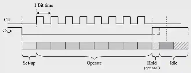
To set up SPI communication on the Raspberry Pi, we need to configure the SPI registers and set up the GPIO pins for SPI functionality. This time I will be using SPI0 Register for SPI communication. The following diagrams1 shows a typical SPI access cycle.
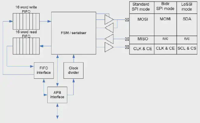
This serial interface peripheral supports the following features:
- Implements a 3 wire serial protocol.
- Implements a 2 wire version of SPI that uses a single wire as a bidirectional data wire instead of one for each direction as in standard SPI.
- Implements a LoSSI Master (Low Speed Serial Interface).
- Provides support for polled, interrupt or DMA operation.
The block diagram that represnts the internal controller is shown below:
I will be using FIFO with 8 bits data size and will be using GPIO 8 as SPI0_CE0_N, GPIO 9 as SPI0_MISO, GPIO 10 as SPI0_MOSI and GPIO 11 as SPI0_SCLK. And polling on SPI CS DONE flag to check the end of transmission. It can also be done by an interrupt but I leave it as self learning for the readers.
The SPI clock can be set using SPIx_CLK register:
$$ \text{SPIx\_CLK} = \frac{\text{system\_clock\_freq}}{2 \times (\text{speed\_field} + 1)} $$
Code Implementation #
Given below is the complete assembly code to set up SPI and send “Hello World” string over SPI at 4MHz SPI clock:
.equ   MPIDR_AFFINITY_MASK, 0x3
.equ   PERIPHERAL_BASE,     0x3F000000
.equ   GPFSEL0,             (PERIPHERAL_BASE + 0x200000)
.equ   GPFSEL1,             (PERIPHERAL_BASE + 0x200004)
.equ   GPPUD,               (PERIPHERAL_BASE + 0x200094)
.equ   GPPUDCLK0,           (PERIPHERAL_BASE + 0x200098)
.equ   SPI0_BASE,           (PERIPHERAL_BASE + 0x204000)
.equ   SPI0_CS,             (SPI0_BASE + 0x00)
.equ   SPI0_FIFO,           (SPI0_BASE + 0x04)
.equ   SPI0_CLK,            (SPI0_BASE + 0x08)
.equ   SPI0_CS_TXD,         (1 << 18)
.equ   SPI0_CS_RXD,         (1 << 17)
.equ   SPI0_CS_DONE,        (1 << 16)
.equ   SPI0_CS_REN,         (1 << 12)
.equ   SPI0_CS_TA,          (1 << 7)
.equ   SPI0_CS_CLEAR_RX,    (1 << 5)
.equ   SPI0_CS_CLEAR_TX,    (1 << 4)

.section ".data"
hello_world_msg:
    .asciz "Hello World\n"
hello_world_msg_end:

.section ".text.boot"
.global _start

_start:
    mrs     x1, mpidr_el1
    and     x1, x1, #MPIDR_AFFINITY_MASK
    cbnz    x1, park_core

master_core_setup:
    ldr     x1, =_start
    mov     sp, x1
    bl      gpio_init_spi
    bl      spi_init

main_loop:
    bl      spi_send_hello_world
    movz    w3, #0x1

delay_loop:
    subs    w3, w3, #1
    bne     delay_loop
    b       main_loop

gpio_init_spi:
    ldr     x1, =GPFSEL0
    ldr     w2, [x1]
    bic     w2, w2, #(7 << 21)
    bic     w2, w2, #(7 << 24)
    bic     w2, w2, #(7 << 27)
    orr     w2, w2, #(4 << 21)
    orr     w2, w2, #(4 << 24)
    orr     w2, w2, #(4 << 27)
    str     w2, [x1]
    ldr     x1, =GPFSEL1
    ldr     w2, [x1]
    bic     w2, w2, #(7 << 0)
    bic     w2, w2, #(7 << 3)
    orr     w2, w2, #(4 << 0)
    orr     w2, w2, #(4 << 3)
    str     w2, [x1]
    ldr     x1, =GPPUD
    mov     w2, #0
    str     w2, [x1]
    mov     x2, #150
wait_pud_1:
    sub     x2, x2, #1
    cbnz    x2, wait_pud_1
    ldr     x1, =GPPUDCLK0
    mov     w2, #0xF80
    str     w2, [x1]
    mov     x2, #150
wait_pud_2:
    sub     x2, x2, #1
    cbnz    x2, wait_pud_2
    mov     w2, #0
    str     w2, [x1]
    ret

spi_init:
    ldr     x1, =SPI0_CS
    mov     w2, #0
    str     w2, [x1]
    mov     w3, #1000
spi_init_wait1:
    subs    w3, w3, #1
    bne     spi_init_wait1
    mov     w2, #(SPI0_CS_CLEAR_RX | SPI0_CS_CLEAR_TX)
    str     w2, [x1]
    mov     w3, #1000
spi_init_wait2:
    subs    w3, w3, #1
    bne     spi_init_wait2
    ldr     x1, =SPI0_CLK
    movz    w2, #64
    str     w2, [x1]
    ret

spi_transfer:
    stp     x29, x30, [sp, #-16]!
    stp     x19, x20, [sp, #-16]!
    stp     x21, x22, [sp, #-16]!
    cbz     x1, transfer_done
    mov     x19, x0
    mov     x20, x1
    ldr     x21, =SPI0_CS
    ldr     x22, =SPI0_FIFO
    mov     w2, #(SPI0_CS_CLEAR_RX | SPI0_CS_CLEAR_TX)
    str     w2, [x21]
    mov     w3, #2
clear_wait:
    subs    w3, w3, #1
    bne     clear_wait
    mov     w2, #SPI0_CS_TA
    str     w2, [x21]
loop_fifo_write:
    cbz     x20, wait_transfer_complete
    ldr     w2, [x21]
    tst     w2, #SPI0_CS_TXD
    beq     loop_fifo_write
    ldrb    w0, [x19], #1
    str     w0, [x22]
    sub     x20, x20, #1
    b       loop_fifo_write
wait_transfer_complete:
    ldr     w2, [x21]
    tst     w2, #SPI0_CS_DONE
    beq     wait_transfer_complete
    bic     w2, w2, #SPI0_CS_TA
    str     w2, [x21]
drain_rx_fifo:
    ldr     w2, [x21]
    tst     w2, #SPI0_CS_RXD
    beq     rx_fifo_empty
    ldr     w0, [x22]
    b       drain_rx_fifo
rx_fifo_empty:
    ldr     w2, [x21]
    orr     w2, w2, #(SPI0_CS_CLEAR_RX | SPI0_CS_CLEAR_TX)
    str     w2, [x21]
transfer_done:
    ldp     x21, x22, [sp], #16
    ldp     x19, x20, [sp], #16
    ldp     x29, x30, [sp], #16
    ret

spi_send_hello_world:
    stp     x29, x30, [sp, #-16]!
    ldr     x0, =hello_world_msg
    ldr     x1, =hello_world_msg_end
    sub     x1, x1, x0
    sub     x1, x1, #1
    bl      spi_transfer
    ldp     x29, x30, [sp], #16
    ret

park_core:
    wfe
    b       park_core
Lets break down the code to understand its functionality: I will be only covering the SPI related functions here. For parking core, system configuration and GPIO setup refer to my previous blog posts
GPIO Initialization for SPI #
The gpio_init_spi function configures the GPIO pins 8, 9, 10, and 11 for SPI functionality by setting their alternate functions. It also disables pull-up/down resistors for these pins. See older blog posts for detailed explanation of GPIO configuration.
SPI Initialization #
This function initializes the SPI0 peripheral by resetting the control/status register, clearing the RX and TX FIFOs, and setting the SPI clock speed to 4MHz (assuming a system clock of 250MHz, the speed field is set to 31).
The register descriptors used in the code are as follows:
SPI0 base Address is 0x3F204000 and all the offsets are from this base address.
| Offset | Name | Description |
|---|---|---|
| 0x00 | CS | SPI Master Control and Status |
| 0x04 | FIFO | SPI Master TX and RX FIFOs |
| 0x08 | CLK | SPI Master Clock Divider |
| 0x0c | DLEN | SPI Master Data Length |
| 0x10 | LTOH | SPI LoSSI mode TOH |
| 0x14 | DC | SPI DMA DREQ Controls |
The most important registers used are SPIO_CS register and SPI0_CLK.
The table below describes the bits of these registers:
SPI CS Register Bits #
| Bits | Name | Description | Type | Reset |
|---|---|---|---|---|
| 31:26 | Reserved | - | - | - |
| 25 | LEN_LONG | Enable Long data word in LoSSI mode if DMA_LEN is set • 0 = Single byte write • 1 = 32-bit word write |
RW | 0x0 |
| 24 | DMA_LEN | Enable DMA mode in LoSSI mode | RW | 0x0 |
| 23 | CSPOL2 | Chip Select 2 Polarity • 0 = Active low • 1 = Active high |
RW | 0x0 |
| 22 | CSPOL1 | Chip Select 1 Polarity • 0 = Active low • 1 = Active high |
RW | 0x0 |
| 21 | CSPOL0 | Chip Select 0 Polarity • 0 = Active low • 1 = Active high |
RW | 0x0 |
| 20 | RXF | RX FIFO Full • 0 = Not full • 1 = Full, no further data will be sent/received |
RO | 0x0 |
| 19 | RXR | RX FIFO needs Reading (¾ full) • 0 = Less than ¾ full • 1 = ¾ or more full |
RO | 0x0 |
| 18 | TXD | TX FIFO can accept Data • 0 = Full • 1 = Has space for at least 1 byte |
RO | 0x1 |
| 17 | RXD | RX FIFO contains Data • 0 = Empty • 1 = Contains at least 1 byte |
RO | 0x0 |
| 16 | DONE | Transfer Done • 0 = In progress • 1 = Complete |
RO | 0x0 |
| 15 | TE_EN | Unused | RW | 0x0 |
| 14 | LMONO | Unused | RW | 0x0 |
| 13 | LEN | LoSSI enable • 0 = SPI master mode • 1 = LoSSI master mode |
RW | 0x0 |
| 12 | REN | Read Enable • 0 = Write to SPI peripheral • 1 = Read from SPI peripheral |
RW | 0x1 |
| 11 | ADCS | Automatically De-assert Chip Select • 0 = Manual control • 1 = Auto de-assert at end of DMA |
RW | 0x0 |
| 10 | INTR | Interrupt on RXR • 0 = No interrupt • 1 = Generate interrupt while RXR = 1 |
RW | 0x0 |
| 9 | INTD | Interrupt on Done • 0 = No interrupt • 1 = Generate interrupt when DONE = 1 |
RW | 0x0 |
| 8 | DMAEN | DMA Enable • 0 = No DMA requests • 1 = Enable DMA operation |
RW | 0x0 |
| 7 | TA | Transfer Active • 0 = Not active, CS lines high • 1 = Active, CS lines set per CS bits |
RW | 0x0 |
| 6 | CSPOL | Chip Select Polarity • 0 = Active low • 1 = Active high |
RW | 0x0 |
| 5:4 | CLEAR | FIFO Clear • 00 = No action • x1 = Clear TX FIFO • 1x = Clear RX FIFO |
W1SC | 0x0 |
| 3 | CPOL | Clock Polarity • 0 = Rest state low • 1 = Rest state high |
RW | 0x0 |
| 2 | CPHA | Clock Phase • 0 = First transition at middle of data bit • 1 = First transition at beginning |
RW | 0x0 |
| 1:0 | CS | Chip Select • 00 = CS0 • 01 = CS1 • 10 = CS2 • 11 = Reserved |
RW | 0x0 |
SPI CLK Register Bits #
| Bits | Name | Description | Type | Reset |
|---|---|---|---|---|
| 31:16 | Reserved | - | - | - |
| 15:0 | CDIV | Clock Divider SCLK = Core Clock / CDIV If CDIV is set to 0, the divisor is 65536. The divisor must be a multiple of 2. Odd numbers rounded down. The maximum SPI clock rate is of the APB clock. |
RW | 0x0000 |
in the initialization section of the code, we clear the SPI0_CS register, wait for some time, clear both RX and TX FIFOs by setting the CLEAR bits, wait again, and finally set the SPI0_CLK register to achieve a 4MHz SPI clock.
spi_init:
    ldr     x1, =SPI0_CS // Load address of SPI0_CS register
    mov     w2, #0       // Prepare to clear the register
    str     w2, [x1]     // Clear SPI0_CS register
    mov     w3, #1000  // Delay loop counter
spi_init_wait1:
    subs    w3, w3, #1  // Decrement counter
    bne     spi_init_wait1 // Wait until counter reaches zero
    mov     w2, #(SPI0_CS_CLEAR_RX | SPI0_CS_CLEAR_TX) // Prepare to clear RX and TX FIFOs
    str     w2, [x1]    // Clear RX and TX FIFOs
    mov     w3, #1000 // Delay loop counter
spi_init_wait2:
    subs    w3, w3, #1  // Decrement counter
    bne     spi_init_wait2 // Wait until counter reaches zero
    ldr     x1, =SPI0_CLK // Load address of SPI0_CLK register
    movz    w2, #64       // Set clock divider for 4MHz SPI clock (assuming 500MHz system clock)
    str     w2, [x1]      // Set SPI0_CLK register
    ret
SPI Transfer #
The spi_transfer function handles the transmission “Hello world!\n” SPI. I will skiip of spi_send_hello_world: function as it is self explanatory.
SPI FIFO Register Bits #
| Bits | Name | Description | Type | Reset |
|---|---|---|---|---|
| 31:0 | DATA | DMA Mode (DMAEN set) If TA is clear, the first 32-bit write to this register will control SPIDLEN and SPICS. Subsequent reads and writes will be taken as four-byte data words to be read/written to the FIFOs Poll/Interrupt Mode (DMAEN clear, TA set) Writes to the register write bytes to TX FIFO. Reads from register read bytes from the RX FIFO |
RW |
0x00000000 |
The crux os the SPI data transfer is handled in spi_transfer function.n
spi_transfer:
    stp     x29, x30, [sp, #-16]!  // Save frame pointer and link register
    stp     x19, x20, [sp, #-16]!  // Save registers x19 and x20
    stp     x21, x22, [sp, #-16]!  // Save registers x21 and x22
    cbz     x1, transfer_done      // If length is zero, skip transfer
    mov     x19, x0                // Move data pointer to x19
    mov     x20, x1                // Move length to x20
    ldr     x21, =SPI0_CS          // Load address of SPI0_CS register
    ldr     x22, =SPI0_FIFO        // Load address of SPI0_FIFO register
    mov     w2, #(SPI0_CS_CLEAR_RX | SPI0_CS_CLEAR_TX) // Prepare to clear RX and TX FIFOs
    str     w2, [x21]              // Clear RX and TX FIFOs
    mov     w3, #2                 // Delay loop counter
clear_wait:
    subs    w3, w3, #1             // Decrement counter
    bne     clear_wait             // Wait until counter reaches zero
    mov     w2, #SPI0_CS_TA        // Prepare to start transfer by setting TA bit
    str     w2, [x21]              // Start transfer by setting TA bit
loop_fifo_write:
    cbz     x20, wait_transfer_complete // If length is zero, wait for transfer to complete
    ldr     w2, [x21]              // Load SPI0_CS register
    tst     w2, #SPI0_CS_TXD       // Test if TX FIFO can accept data
    beq     loop_fifo_write        // If TX FIFO is full, wait
    ldrb    w0, [x19], #1          // Load byte from data pointer and increment pointer
    str     w0, [x22]              // Write byte to SPI0_FIFO
    sub     x20, x20, #1           // Decrement length
    b       loop_fifo_write        // Repeat for next byte
wait_transfer_complete:
    ldr     w2, [x21]              // Load SPI0_CS register
    tst     w2, #SPI0_CS_DONE      // Test if transfer is done
    beq     wait_transfer_complete // Wait until transfer is done
    bic     w2, w2, #SPI0_CS_TA   // Clear TA bit to end transfer
    str     w2, [x21]              // Write back to SPI0_CS register
drain_rx_fifo:
    ldr     w2, [x21]            // Load SPI0_CS register
    tst     w2, #SPI0_CS_RXD    // Test if RX FIFO contains data
    beq     rx_fifo_empty      // If RX FIFO is empty, skip draining
    ldr     w0, [x22]          // Read byte from SPI0_FIFO (discarded)
    b       drain_rx_fifo        // Repeat until RX FIFO is emptyy
rx_fifo_empty:
    ldr     w2, [x21]               // Load SPI0_CS register
    orr     w2, w2, #(SPI0_CS_CLEAR_RX | SPI0_CS_CLEAR_TX) // Prepare to clear RX and TX FIFOs
    str     w2, [x21]              // Clear RX and TX FIFOs
transfer_done:
    ldp     x21, x22, [sp], #16   // Restore registers x21 and x22
    ldp     x19, x20, [sp], #16   // Restore registers x19 and x20
    ldp     x29, x30, [sp], #16   // Restore frame pointer and link register
    ret
The sequence diagram below shows a SPI data transfer implemented in this blog (right click and open in new tab for detailed view):

Final result #
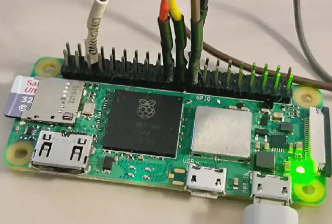
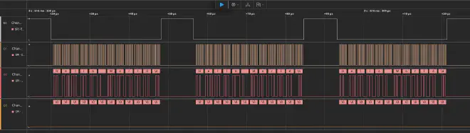
I hooked the GPIO8, GPIO9, GPIO10, and GPIO11 pins to an logic analyzer as shown in figure below to capture the SPI signals. I could achieve 4 MHz SPI clock frequency sensing Hello World\n in a loop.
The whole packet takes 28.188 µs for the transfer of 12 bytes that is a throughput of approximately 3.4 Mbps of throughput. I could try to enable DMA in future but for now here is the output capture:
Right click and open in new tab for detailed view:
I may not be able to create a frequent series of Raspberry Pi bare bone tutorials due to time constraints and personal family commitments, but I will try to post more articles whenever possible. Stay tuned for more updates!