Raspberry PI Bare Metal Vol 5 : PWM Sine Wave Generator #
In my previous blog post I implemented timer functionality on the Raspberry Pi. In this post, I will combine PWM (Pulse Width Modulation) with timers to generate a sine wave output.
PWM (Pulse Width Modulation) Overview #
Pulse Width Modulation is a technique where we vary the duty cycle of a square wave to encode information. By rapidly changing the duty cycle according to a sine lookup table, and filtering the output with a simple RC low-pass filter, we can generate an analog sine wave. If you know FM modulation from communication systems, PWM is similar in concept.
The Raspberry Pi Zero 2W has two PWM channels:
- PWM0 on GPIO 12, 18
- PWM1 on GPIO 13, 19
I will be using GPIO 18 for PWM0 in this tutorial.
PWM Registers #
The PWM base address is 0x3F20C000 and all offsets are from this base address.
| Offset | Name | Description |
|---|---|---|
| 0x00 | CTL | PWM Control |
| 0x04 | STA | PWM Status |
| 0x08 | DMAC | PWM DMA Configuration |
| 0x10 | RNG1 | PWM Channel 1 Range |
| 0x14 | DAT1 | PWM Channel 1 Data |
| 0x18 | FIF1 | PWM FIFO Input |
| 0x20 | RNG2 | PWM Channel 2 Range |
| 0x24 | DAT2 | PWM Channel 2 Data |
CTL Register Bits #
| Bits | Name | Description | Type | Reset |
|---|---|---|---|---|
| 15 | MSEN2 | Channel 2 M/S Enable • 0 = PWM algorithm • 1 = M/S transmission |
RW | 0x0 |
| 13 | USEF2 | Channel 2 Use FIFO • 0 = Data register • 1 = FIFO |
RW | 0x0 |
| 12 | POLA2 | Channel 2 Polarity • 0 = Normal • 1 = Inverted |
RW | 0x0 |
| 11 | SBIT2 | Channel 2 Silence Bit | RW | 0x0 |
| 10 | RPTL2 | Channel 2 Repeat Last Data | RW | 0x0 |
| 9 | MODE2 | Channel 2 Mode • 0 = PWM mode • 1 = Serialiser mode |
RW | 0x0 |
| 8 | PWEN2 | Channel 2 Enable | RW | 0x0 |
| 7 | MSEN1 | Channel 1 M/S Enable • 0 = PWM algorithm • 1 = M/S transmission |
RW | 0x0 |
| 6 | CLRF1 | Clear FIFO | W1C | 0x0 |
| 5 | USEF1 | Channel 1 Use FIFO | RW | 0x0 |
| 4 | POLA1 | Channel 1 Polarity | RW | 0x0 |
| 3 | SBIT1 | Channel 1 Silence Bit | RW | 0x0 |
| 2 | RPTL1 | Channel 1 Repeat Last Data | RW | 0x0 |
| 1 | MODE1 | Channel 1 Mode | RW | 0x0 |
| 0 | PWEN1 | Channel 1 Enable | RW | 0x0 |
Clock Manager #
The PWM clock must be configured separately using the Clock Manager. The Clock Manager base is at 0x3F1010A0 for PWM.
| Offset | Name | Description |
|---|---|---|
| 0x00 | CM_PWMCTL | Clock Manager PWM Control |
| 0x04 | CM_PWMDIV | Clock Manager PWM Divisor |
The clock password is 0x5A and must be written to bits 31:24 for any write operation.
CM_PWMCTL Register Bits #
| Bits | Name | Description |
|---|---|---|
| 31:24 | PASSWD | Clock Manager password (0x5A) |
| 7 | BUSY | Clock generator is running |
| 4 | ENAB | Enable the clock generator |
| 3:0 | SRC | Clock source (6 = PLLD @ 500MHz) |
CM_PWMDIV Register Bits #
| Bits | Name | Description |
|---|---|---|
| 31:24 | PASSWD | Clock Manager password (0x5A) |
| 23:12 | DIVI | Integer part of divisor |
| 11:0 | DIVF | Fractional part of divisor |
Sine Wave Generation Theory #
To generate a sine wave using PWM:
- Create a lookup table with pre-calculated sine values
- Use a timer to step through the table at regular intervals
- Update the PWM duty cycle with the current sine value
- Filter the PWM output with an RC low-pass filter
The output frequency is determined by:
$$ f_{\text{out}} = \frac{f_{\text{sample}}}{N_{\text{samples}}} $$
Where $$ f_{\text{sample}} \text{ is the rate at which we update the PWM value, and } $$ $$N_{\text{samples}} \text{ is the number of entries in our sine table.} $$
For a 1kHz sine wave with 64 samples:
$$ f_{\text{sample}} = 1000 \times 64 = 64000 \text{ Hz} $$
Code Implementation #
Below is the complete assembly code to generate a sine wave using PWM:
.equ   MPIDR_AFFINITY_MASK, 0x3
.equ   PERIPHERAL_BASE,     0x3F000000
.equ   GPFSEL1,             (PERIPHERAL_BASE + 0x200004)
.equ   TIMER_BASE,          (PERIPHERAL_BASE + 0x003000)
.equ   TIMER_CS,            (TIMER_BASE + 0x00)
.equ   TIMER_CLO,           (TIMER_BASE + 0x04)
.equ   TIMER_C1,            (TIMER_BASE + 0x10)
.equ   IRQ_BASE,            (PERIPHERAL_BASE + 0xB000)
.equ   IRQ_PENDING_1,       (IRQ_BASE + 0x204)
.equ   IRQ_ENABLE_1,        (IRQ_BASE + 0x210)
.equ   LOCAL_BASE,          0x40000000
.equ   CORE0_TIMER_IRQCNTL, (LOCAL_BASE + 0x40)
.equ   TIMER_IRQ_1,         (1 << 1)
.equ   PWM_BASE,            (PERIPHERAL_BASE + 0x20C000)
.equ   PWM_CTL,             (PWM_BASE + 0x00)
.equ   PWM_RNG1,            (PWM_BASE + 0x10)
.equ   PWM_DAT1,            (PWM_BASE + 0x14)
.equ   CM_BASE,             (PERIPHERAL_BASE + 0x101000)
.equ   CM_PWMCTL,           (CM_BASE + 0x0A0)
.equ   CM_PWMDIV,           (CM_BASE + 0x0A4)
.equ   CM_PASSWD,           0x5A000000
.equ   PWM_CTL_MSEN1,       (1 << 7)
.equ   PWM_CTL_PWEN1,       (1 << 0)
.equ   PWM_CTL_CLRF1,       (1 << 6)

.equ   SINE_TABLE_SIZE,     256
.equ   PWM_RANGE,           1024
.equ   SAMPLE_INTERVAL_US,  30     // 256 samples * 30us ≈ 7.68ms period = ~130Hz sine wave

.section ".data"
.align 4
sine_index:
    .word 0

sine_table:
    .word 512, 525, 537, 550, 562, 575, 587, 599
    .word 612, 624, 636, 648, 660, 672, 684, 696
    .word 708, 719, 730, 742, 753, 764, 775, 785
    .word 796, 806, 816, 826, 836, 846, 855, 864
    .word 873, 882, 891, 899, 907, 915, 922, 930
    .word 937, 944, 950, 957, 963, 968, 974, 979
    .word 984, 989, 993, 997, 1001, 1004, 1008, 1011
    .word 1013, 1015, 1017, 1019, 1021, 1022, 1022, 1023
    .word 1023, 1023, 1022, 1022, 1021, 1019, 1017, 1015
    .word 1013, 1011, 1008, 1004, 1001, 997, 993, 989
    .word 984, 979, 974, 968, 963, 957, 950, 944
    .word 937, 930, 922, 915, 907, 899, 891, 882
    .word 873, 864, 855, 846, 836, 826, 816, 806
    .word 796, 785, 775, 764, 753, 742, 730, 719
    .word 708, 696, 684, 672, 660, 648, 636, 624
    .word 612, 599, 587, 575, 562, 550, 537, 525
    .word 512, 499, 487, 474, 462, 449, 437, 425
    .word 412, 400, 388, 376, 364, 352, 340, 328
    .word 316, 305, 294, 282, 271, 260, 249, 239
    .word 228, 218, 208, 198, 188, 178, 169, 160
    .word 151, 142, 133, 125, 117, 109, 102,  94
    .word  87,  80,  74,  67,  61,  56,  50,  45
    .word  40,  35,  31,  27,  23,  20,  16,  13
    .word  11,   9,   7,   5,   3,   2,   2,   1
    .word   1,   1,   2,   2,   3,   5,   7,   9
    .word  11,  13,  16,  20,  23,  27,  31,  35
    .word  40,  45,  50,  56,  61,  67,  74,  80
    .word  87,  94, 102, 109, 117, 125, 133, 142
    .word 151, 160, 169, 178, 188, 198, 208, 218
    .word 228, 239, 249, 260, 271, 282, 294, 305
    .word 316, 328, 340, 352, 364, 376, 388, 400
    .word 412, 425, 437, 449, 462, 474, 487, 499

.section ".text.boot"
.global _start

_start:
    mrs     x1, mpidr_el1
    and     x1, x1, #MPIDR_AFFINITY_MASK
    cbnz    x1, park_core
    ldr     x1, =_start
    mov     sp, x1
    mov     x0, #(1 << 31)
    orr     x0, x0, #(1 << 4)
    orr     x0, x0, #(1 << 3)
    msr     hcr_el2, x0
    ldr     x0, =vector_table
    msr     vbar_el2, x0
    bl      gpio_init_pwm
    bl      pwm_clock_init
    bl      pwm_init
    bl      timer_init
    msr     daifclr, #2

main_loop:
    wfi
    b       main_loop

.balign 0x800
vector_table:
    b       hang
    .balign 0x80
    b       irq_handler
    .balign 0x80
    b       hang
    .balign 0x80
    b       hang
    .balign 0x80
    b       hang
    .balign 0x80
    b       irq_handler
    .balign 0x80
    b       hang
    .balign 0x80
    b       hang
    .balign 0x80
    b       hang
    .balign 0x80
    b       hang
    .balign 0x80
    b       hang
    .balign 0x80
    b       hang
    .balign 0x80
    b       hang
    .balign 0x80
    b       hang
    .balign 0x80
    b       hang
    .balign 0x80
    b       hang
    .balign 0x80
    b       hang

hang:
    wfe
    b       hang

irq_handler:
    stp     x0, x1, [sp, #-16]!
    stp     x2, x3, [sp, #-16]!
    stp     x29, x30, [sp, #-16]!
    ldr     x0, =IRQ_PENDING_1
    ldr     w1, [x0]
    tst     w1, #TIMER_IRQ_1
    beq     irq_done
    ldr     x0, =TIMER_CS
    mov     w1, #(1 << 1)
    str     w1, [x0]
    ldr     x0, =sine_index
    ldr     w1, [x0]
    ldr     x2, =sine_table
    lsl     w3, w1, #2
    ldr     w3, [x2, x3]
    ldr     x2, =PWM_DAT1
    str     w3, [x2]
    add     w1, w1, #1
    and     w1, w1, #(SINE_TABLE_SIZE - 1)
    str     w1, [x0]
    ldr     x0, =TIMER_CLO
    ldr     w1, [x0]
    add     w1, w1, #SAMPLE_INTERVAL_US
    ldr     x0, =TIMER_C1
    str     w1, [x0]
irq_done:
    ldp     x29, x30, [sp], #16
    ldp     x2, x3, [sp], #16
    ldp     x0, x1, [sp], #16
    eret

gpio_init_pwm:
    ldr     x1, =GPFSEL1
    ldr     w2, [x1]
    bic     w2, w2, #(7 << 24)
    orr     w2, w2, #(2 << 24)
    str     w2, [x1]
    ret

pwm_clock_init:
    ldr     x1, =CM_PWMCTL
    ldr     w2, =CM_PASSWD
    orr     w2, w2, #(1 << 5)
    str     w2, [x1]
clock_wait_stop:
    ldr     w2, [x1]
    tst     w2, #(1 << 7)
    bne     clock_wait_stop
    ldr     x1, =CM_PWMDIV
    ldr     w2, =CM_PASSWD
    mov     w3, #100
    lsl     w3, w3, #12
    orr     w2, w2, w3
    str     w2, [x1]
    ldr     x1, =CM_PWMCTL
    ldr     w2, =CM_PASSWD
    orr     w2, w2, #6
    str     w2, [x1]
    ldr     w2, =CM_PASSWD
    orr     w2, w2, #6
    orr     w2, w2, #(1 << 4)
    str     w2, [x1]
clock_wait_start:
    ldr     w2, [x1]
    tst     w2, #(1 << 7)
    beq     clock_wait_start
    ret

pwm_init:
    ldr     x1, =PWM_CTL
    mov     w2, #0
    str     w2, [x1]
    mov     w3, #100
pwm_delay1:
    subs    w3, w3, #1
    bne     pwm_delay1
    mov     w2, #PWM_CTL_CLRF1
    str     w2, [x1]
    ldr     x1, =PWM_RNG1
    mov     w2, #PWM_RANGE
    str     w2, [x1]
    ldr     x1, =PWM_DAT1
    mov     w2, #512
    str     w2, [x1]
    ldr     x1, =PWM_CTL
    mov     w2, #(PWM_CTL_MSEN1 | PWM_CTL_PWEN1)
    str     w2, [x1]
    ret

timer_init:
    ldr     x0, =CORE0_TIMER_IRQCNTL
    mov     w1, #0
    str     w1, [x0]
    ldr     x0, =TIMER_CS
    mov     w1, #0xF
    str     w1, [x0]
    ldr     x0, =TIMER_CLO
    ldr     w1, [x0]
    add     w1, w1, #SAMPLE_INTERVAL_US
    ldr     x0, =TIMER_C1
    str     w1, [x0]
    ldr     x0, =IRQ_ENABLE_1
    mov     w1, #TIMER_IRQ_1
    str     w1, [x0]
    ret

.section ".text"
park_core:
    wfe
    b       park_core
Code Breakdown #
GPIO Configuration for PWM #
GPIO 18 must be set to ALT5 function to enable PWM0 output:
gpio_init_pwm:
    ldr     x1, =GPFSEL1
    ldr     w2, [x1]
    bic     w2, w2, #(7 << 24)       // Clear bits 24-26 for GPIO 18
    orr     w2, w2, #(2 << 24)       // Set ALT5 (PWM0) for GPIO 18
    str     w2, [x1]
    ret
PWM Clock Configuration #
The PWM peripheral requires a separate clock configuration. We use PLLD (100MHz) divided by 100 to get a 5MHz PWM clock:
pwm_clock_init:
    // Stop the clock first
    ldr     x1, =CM_PWMCTL
    ldr     w2, =CM_PASSWD
    orr     w2, w2, #(1 << 5)        // Kill bit
    str     w2, [x1]
    ...
    ...
    // Set divisor: 500MHz / 100 = 5MHz
    ldr     x1, =CM_PWMDIV
    ldr     w2, =CM_PASSWD
    mov     w3, #100
    lsl     w3, w3, #12
    ...
    ...
    // Enable with PLLD source
    ldr     x1, =CM_PWMCTL
    ldr     w2, =CM_PASSWD
    orr     w2, w2, #6
    orr     w2, w2, #(1 << 4)
    str     w2, [x1]
clock_wait_start:
    ldr     w2, [x1]
    tst     w2, #(1 << 7)
    beq     clock_wait_start
    ret
Sine Wave Generation #
The code above uses a timer interrupt to update the PWM duty cycle with the next value from the sine lookup table, ensuring precise timing and efficient CPU usage. The interrupt handler performs the following steps:
I will not discuss the entire interrupt handler again as it is covered in my previous blog post, but the key steps are:
- Check if the timer interrupt is pending
- Clear the interrupt flag
- Load the current sine index and fetch the corresponding sine value
- Update the PWM data register with the sine value
- Increment the sine index
This approach is implemented in the irq_handler routine in the main assembly code:
irq_handler:
    stp     x0, x1, [sp, #-16]!
    stp     x2, x3, [sp, #-16]!
    stp     x29, x30, [sp, #-16]!
    ldr     x0, =IRQ_PENDING_1
    ldr     w1, [x0]
    tst     w1, #TIMER_IRQ_1
    beq     irq_done
    ldr     x0, =TIMER_CS
    mov     w1, #(1 << 1)
    str     w1, [x0]
    ldr     x0, =sine_index   // Load sine index
    ldr     w1, [x0]
    ldr     x2, =sine_table   // Load sine table base
    lsl     w3, w1, #2     // Calculate offset
    ldr     w3, [x2, x3]  // Fetch sine value
    ldr     x2, =PWM_DAT1  // Load PWM data register address
    str     w3, [x2]       // Update PWM duty cycle
    add     w1, w1, #1
    and     w1, w1, #(SINE_TABLE_SIZE - 1)
    str     w1, [x0]
    ldr     x0, =TIMER_CLO
    ldr     w1, [x0]
    add     w1, w1, #SAMPLE_INTERVAL_US
    ldr     x0, =TIMER_C1
    str     w1, [x0]
irq_done:
    ldp     x29, x30, [sp], #16
    ldp     x2, x3, [sp], #16
    ldp     x0, x1, [sp], #16
    eret
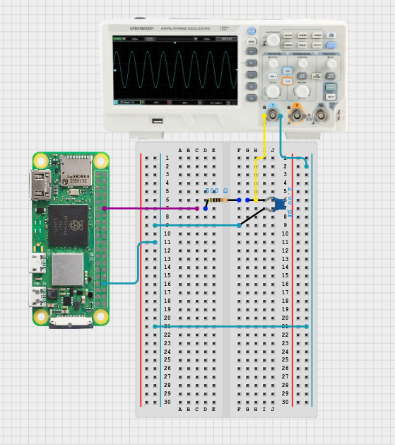
Hardware Setup #
To convert the PWM signal to an analog sine wave, connect a simple RC low-pass filter to GPIO 18 as shown below:
$$ f_c = \frac{1}{2\pi RC} = \frac{1}{2\pi \times 500 \times 1 \times 10^{-6}} \approx 318 \text{ Hz} $$
Adjusting Frequency #
To change the output sine wave frequency, modify the SAMPLE_PERIOD_US constant:
| Sample Period (µs) | Sample Rate (Hz) | Output Frequency (Hz) |
|---|---|---|
| 15 | 66,667 | ~260 |
| 30 | 33,333 | ~130 |
| 62 | 16,129 | ~63 |
| 156 | 6,410 | ~25 |
You can also play around with the SINE_TABLE_SIZE to adjust the number of samples per cycle for different frequencies.
Example Output Frequencies for Different Table Sizes (30 µs Sample Period) #
| Sine Table Size | Sample Period (µs) | Sample Rate (Hz) | Output Frequency (Hz) |
|---|---|---|---|
| 32 | 30 | 33,333 | ~1,042 |
| 64 | 30 | 33,333 | ~521 |
| 128 | 30 | 33,333 | ~260 |
| 256 | 30 | 33,333 | ~130 |
| 512 | 30 | 33,333 | ~65 |
Calculation:
$$ f_{\text{out}} = \frac{f_{\text{sample}}}{N_{\text{samples}}} $$
For example, with a table size of 128: $$ f_{\text{out}} = \frac{33,333}{128} \approx 260,\text{Hz} $$
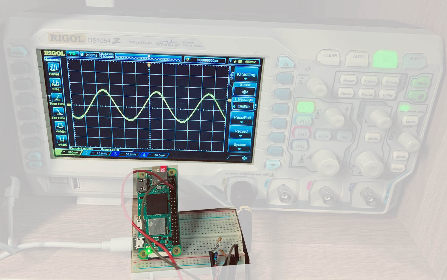
Final Results #
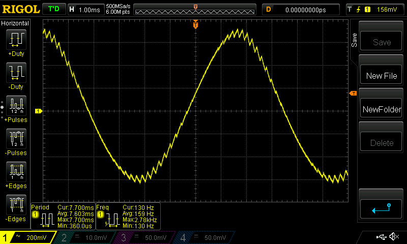
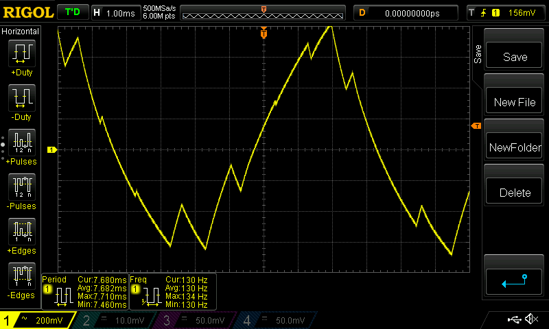
After connecting the RC filter and running the code, you should see a clean sine wave on an oscilloscope. The PWM-generated sine wave at 124 Hz with 256 samples per cycle provides a smooth output.
NOw the theortical and practical results doest align as expected. The expected value was around 130 Hz. The issue is interrupt service routine (ISR) overhead causing the actual frequency to be lower than the theoretical calculation. The SAMPLE_INTERVAL_US is 30µs as intented, but the time taken to handle the interrupt and update the PWM value adds extra delay, resulting in a longer effective period for the sine wave.We have
SINE_TABLE_SIZE of 256 samples which means
$$
Period = 256 × 30µs = 7680µs = 7.68ms
$$
$$ Expected frequency = 1 / 0.00768s \approx 130 \text{ Hz} $$
By the time you read TIMER_CLO and schedule the next interrupt, the timer has already advanced by ~1.5-2µs. This adds up over 256 samples: $$ 256 × ~1.9µs \text { } overhead \approx 480µs \text { } extra \text { } per \text { } cycle $$ $$ Actual period ≈ 7680 + 480 = 1 / 8160µs \approx 124 \text{ Hz} $$
Now in my previous blog it was a simple ISR with large TIMER_INTERVAL which made the overhead negligible. But with high-frequency updates SAMPLE_INTERVAL_US of 30µs, the ISR overhead becomes significant.
To fix the drift we can use a different approach like using a free-running timer and calculating the next interrupt time based on the initial start time plus multiples of SAMPLE_INTERVAL_US. This way, we avoid cumulative errors from ISR overhead.
The ISR code will change to:
irq_handler:
    stp     x0, x1, [sp, #-16]!
    stp     x2, x3, [sp, #-16]!
    stp     x29, x30, [sp, #-16]!
    ldr     x0, =IRQ_PENDING_1
    ldr     w1, [x0]
    tst     w1, #TIMER_IRQ_1
    beq     irq_done
    ldr     x0, =TIMER_CS
    mov     w1, #(1 << 1)
    str     w1, [x0]
    ldr     x0, =sine_index
    ldr     w1, [x0]
    ldr     x2, =sine_table
    lsl     w3, w1, #2
    ldr     w3, [x2, x3]
    ldr     x2, =PWM_DAT1
    str     w3, [x2]
    add     w1, w1, #1
    and     w1, w1, #(SINE_TABLE_SIZE - 1)
    str     w1, [x0]
    ldr     x0, =TIMER_C1
    ldr     w1, [x0]
    add     w1, w1, #SAMPLE_INTERVAL_US
    str     w1, [x0]
irq_done:
    ldp     x29, x30, [sp], #16
    ldp     x2, x3, [sp], #16
    ldp     x0, x1, [sp], #16
    eret
in this new approach, we read the current TIMER_C1 value (which holds the next scheduled interrupt time) and simply add SAMPLE_INTERVAL_US to it for the next interrupt. This way, even if there is some overhead in the ISR, it does not accumulate over time.
ldr     x0, =TIMER_C1      // Load address of the target register
ldr     w1, [x0]             // Get PREVIOUS target time
add     w1, w1, #SAMPLE_INTERVAL_US // Add interval to the old target
str     w1, [x0]            // Update target time
I tested the new approach and achieved a more accurate output frequency closer to the theoretical value as shown in the oscilloscope screenshot below.
There is a pitfall for this approach. i.e It is dangerous if the ISR takes too long to execute. If TIMER_CLO (the actual clock) has already passed the value of previous_Target + interval before you finish the str instruction, the timer will not trigger until the 32-bit counter wraps all the way around (which takes about 71 minutes at 1MHz Timer frequency).
I also changed the PWM frequency to 50 MHz (divisor of 10) to get a cleaner sine wave output.
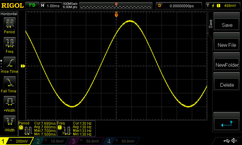
compared to the previous output, the sine wave is much smoother with less ripple due to the higher PWM frequency.
This is 1 MHz PWM sine wave output using the same method:
Making the PWM frequency higher reduces the step size of the PWM waveform, resulting in a smoother analog output after filtering.
Conclusion #
The PWM sine wave generator on Raspberry Pi demonstrates how to leverage PWM and timers to create analog waveforms in a bare-metal environment. This output can be used for various applications such as audio synthesis, signal generation, and motor control. Its a powerful techique that is used when the expensive DACs are not available.
Stay tuned for more such Raspberry Pi bare metal tutorials where we’ll explore other peripherals and applications!